Researchers at the Georgia Institute of Technology in the US have created the world's first functional semiconductor made from graphene. The breakthrough opens the door to the development of entirely new electronic products. The research is published in the journal Nature.
Graphene
Graphene is a single-layer, two-dimensional material composed of carbon atoms with excellent electronic, optical, and mechanical properties. However, the application of pure graphene is subject to some limitations, such as its zero bandgap and difficulty in preparing large-area films. Functionalized graphene expands its applications by introducing different atoms or molecules to interact with graphene, which can modulate its properties and functions. New advances in research on the application of functionalized graphene in different fields. World’s first, functional semiconductor prepared from graphene with electron mobility 10 times higher than silicon.

Semiconductors: Graphene Can Replace Silicon
It was clear from the start that graphene could be miniaturized compared to silicon, making smaller devices possible,” says GaTech researcher Walter de Heer. At the same time, it offers higher processing speeds and generates less unwanted heat,” and “in principle, more components can be packaged on a single graphene chip than with silicon. The technology is also compatible with conventional microelectronics manufacturing, a requirement for any viable silicon alternative.
To create the new nanoelectronics platform, the researchers designed a modified form of inscription on a silicon carbide crystal substrate. In collaboration with researchers at the Tianjin International Centre for Nanoparticles and Nanosystems at Tianjin University, the scientists produced electronic-grade silicon carbide chips.De Heers fabricated graphene in his lab at Georgia Tech using the newly developed oven.

Electrons Create Nanostructures
The researchers used electron beam lithography. This is a method commonly used in microelectronics to write nanostructures in graphene and solder their edges to silicon carbide chips. The process mechanically stabilizes and seals the edges of graphene, which would otherwise react with oxygen and other gases and destroy the chip.
The charges the team observed at the edges of the graphene were similar to those in an optical fiber where photons travel over tens of thousands of nanometres without scattering. This means that all the electricity could be used to work on future chips. Graphene electrons in previous technologies could only travel about ten nanometres before hitting small defects and scattering in different directions.
Graphene is a single sheet of carbon atoms held together by the strongest known bonds. Semiconductors are materials that conduct electricity under certain conditions and are essential components of electronic devices. A long-standing problem in graphene electronics is that graphene does not have the right bandgap and does not turn on and off at the right ratio. Many attempts have been made over the years to solve this problem in various ways. The latest technology enables bandgap, which is a crucial step in the development of graphene-based electronics.

Electron Mobility is 10 Times that of Silicon
The research team made a breakthrough when they used a special furnace to grow graphene on silicon carbide wafers. They produced epitaxial graphene, which is a single layer grown on a silicon carbide wafer. It was found that when properly fabricated, epitaxial graphene chemically bonds with silicon carbide and begins to exhibit semiconductor properties.
However, to fabricate functional transistors, the semiconductor material must be manipulated extensively, which can impair its performance. To prove that their platform could function as a viable semiconductor, the team needed to measure its electronic properties without damaging it.
They placed atoms on graphene and used doping techniques to “donate” electrons to the system, which was used to see if the material was a good conductor. Measurements showed that their graphene semiconductor had a mobility of 10 times that of silicon. In other words, electrons move with very low resistance, which in electronics means faster calculations. The researchers say it’s like driving on a gravel road versus a motorway. It’s more efficient, doesn’t heat up as much, and has a higher velocity so electrons can move faster.
The new development is currently the only 2D semiconductor with all the necessary properties for use in nanoelectronics, and its electrical properties are far superior to any other 2D semiconductor currently under development. The researchers say that epitaxial graphene could cause a paradigm shift in electronics and lead to entirely new technologies that take advantage of its unique properties. The material permits the exploitation of the quantum mechanical wave properties of electrons, thus meeting the requirements of quantum computing.
Applications of Functionalized Graphene in Electronic Devices
Functionalized graphene has a wide range of applications in electronic devices, and this section will focus on its applications in transistors and integrated circuits, flexible electronic devices, sensors and detectors, and optoelectronic devices.
- Transistors and integrated circuits: Graphene has excellent electron transport properties and can be used as a transistor material for high-speed electronic devices. Functionalized graphene can modulate its conductive properties by introducing dopant atoms or molecules, such as boron, nitrogen, and phosphorus. For example, nitrogen-doped graphene has p-type semiconductor properties and can be used to construct p-n structure transistors.
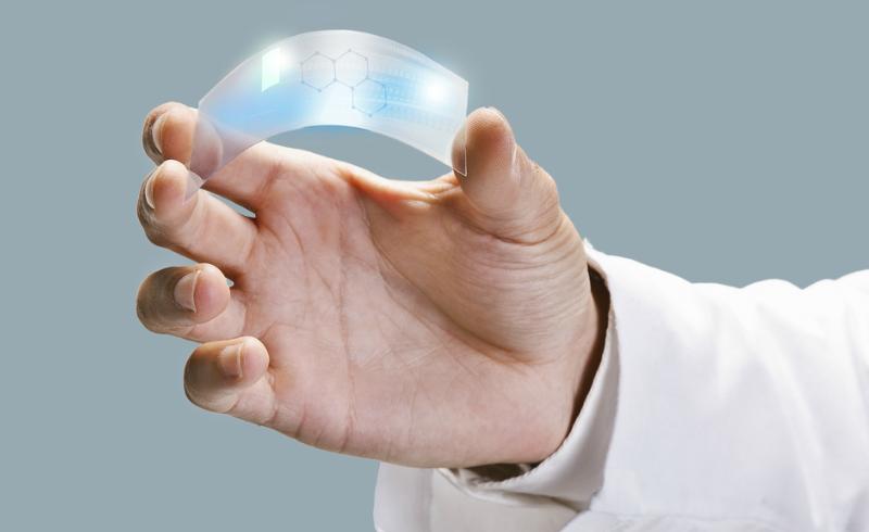
- Flexible electronic devices: Due to the flexible and thin film nature of graphene, functionalized graphene has a wide range of potential applications in flexible electronic devices. For example, graphene films can be used as transparent conductive films for flexible display devices and touch screens.
- Sensors and detectors: Functionalized graphene has excellent performance in the field of sensors and detectors. Due to its high surface area and high sensitivity, graphene can be used in gas sensors, chemical sensors, and biosensors, among others. By introducing specific functional groups or molecules, graphene can be made highly selective and sensitive to target substances, achieving high-performance sensors and detectors.


Your point of view caught my eye and was very interesting. Thanks. I have a question for you.