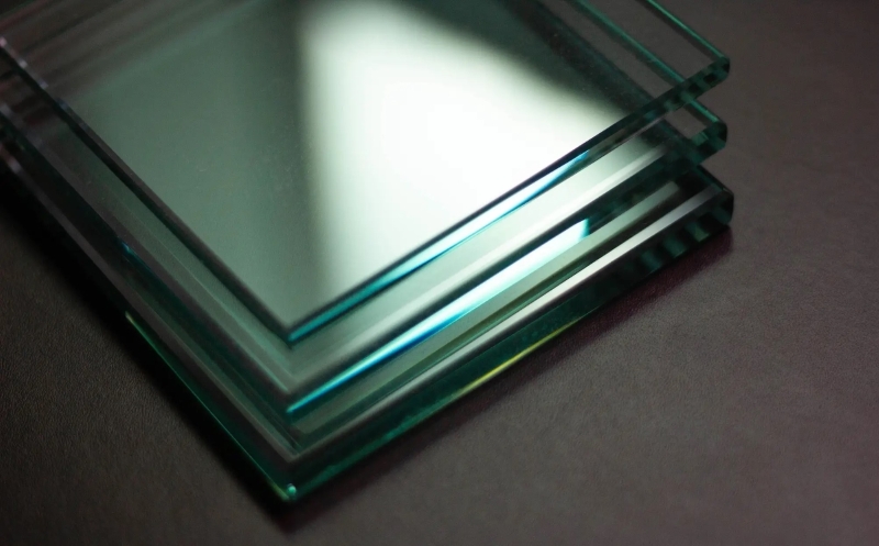
As the semiconductor industry’s demand for chips with higher integration and better performance continues to surge, traditional glass materials are undergoing a transformative evolution. From being a “supporting role” in only a few specific processes, they have grown into a strategic platform supporting semiconductor manufacturing and advanced packaging. According to a report by Yole Group, glass materials have been deeply integrated into multiple terminal fields such as CIS, memory/HBM, and AR/VR, and their market scale and technological influence will achieve leapfrog growth in the next five years.
From Specialized to Fundamental: The Strategic Transformation of Glass Materials
For a long time, the application scenarios of glass in the semiconductor industry have been limited. However, the rapid advancement of technologies such as 3D packaging and advanced manufacturing processes has fully activated its strategic value. Currently, carrier wafers remain the main source of revenue for glass materials, but the importance of functional applications such as wafer-level optics, panel substrates, glass core substrates, and TGV (Through-Glass Via) interconnection is rising rapidly.
Yole Group predicts that from 2025 to 2030, the demand for glass wafers in the semiconductor field will grow at a compound annual growth rate (CAGR) of 10.2%, higher than the revenue growth. The core drivers come from the popularization of multiple bonding processes and the transformation of packaging technology from 2D to 3D. By 2030, the global demand for semiconductor glass materials is expected to be nearly three times the current level, with CIS, microfluidics, power devices, memory/HBM and other fields becoming the main growth engines.

Coexistence of Core Advantages and Popularization Challenges
The rise of glass materials stems from their unique properties that perfectly meet the needs of advanced manufacturing. Compared with traditional silicon interposers and organic substrates, glass has a lower coefficient of thermal expansion, which can significantly improve the warpage problem in multi-chip packaging. At the same time, its flatness advantage can simplify the lithography process, making it possible to achieve redistribution layers (RDL) with line widths and spacing less than 2 microns. In high-frequency and high-speed application scenarios, glass has more prominent advantages. Its dielectric constant is much lower than that of silicon, and its tangent loss is relatively low. The transmission loss is several orders of magnitude lower than that of silicon, which can greatly improve signal integrity, making it an ideal material for cutting-edge fields such as 6G communication.
In the field of microfluidics, the dimensional stability and chemical resistance of glass have made it occupy nearly a quarter of the market share; in the memory field, through the application of a number of key technologies, glass has promoted the performance improvement of HBM devices, and the compound annual growth rate of this field from 2025 to 2030 is as high as 33%. In terms of cost control, glass materials also show great potential. With the maturity of technology, glass recycling and multi-cycle reuse have gradually become the mainstream practice in the industry, effectively reducing the single-cycle cost and further enhancing its market competitiveness.

However, the full popularization of glass materials in the semiconductor field still faces multiple obstacles. Technically, the inevitable microcrack problem during glass cutting and the mass production challenge of high-aspect-ratio TGV have become core bottlenecks restricting their large-scale application. At present, TGV manufacturing mainly relies on the combination of laser modification and hydrofluoric acid etching. Although the processing of 3-micron apertures has been achieved, there is still room for improvement in stability and environmental protection. The industry is actively exploring hydrofluoric acid-free etching solutions. High equipment dependence is also an important challenge. The equipment performance in links such as temporary bonding/debonding, via formation, CMP (Chemical Mechanical Polishing), metrology, and carrier cleaning directly determines the production capacity and yield of glass material applications. The Yole Group report points out that these equipment links have become key constraints to industry development, requiring in-depth collaborative innovation between material suppliers and equipment manufacturers.
On the supply chain front, the global semiconductor glass material market is highly concentrated. By 2025, the four giants—AGC, PlanOptik, Corning, and Schott—will account for approximately 90% of the revenue share, posing high technical and capital barriers for new entrants. Meanwhile, the supply chain is undergoing structural restructuring, with regional redundancy layout, high specification, and contractual cooperation emerging as the latest industry trend, which places higher requirements on enterprises’ production capacity control and localized service capabilities.
Faced with these challenges, the supply chain of semiconductor glass materials is accelerating its transformation. Yole Group predicts that by 2030, this supply chain will gradually show similar characteristics to the IC substrate industry, with three core trends: improved regional redundancy capabilities, higher specification, and increased contractualization. This transformation is driven not only by local incentive policies and risk management needs but also by downstream customers’ strict requirements for key indicators such as tolerance and flatness. Long-term cooperation is shifting from focusing on single-chip prices to single-cycle cost control.
The rise of glass materials is an inevitable result of the coordinated development of materials science and advanced manufacturing technology, becoming an important support for the semiconductor industry to move towards higher performance, smaller size, and lower power consumption. Although challenges remain, with continuous industry investment, relevant issues will be gradually resolved. In the next ten years, all industry stakeholders need to actively adapt to supply chain changes, strengthen technological innovation and cross-border cooperation to seize opportunities in this industrial transformation. Glass materials will continue to inject strong momentum into the innovative development of the semiconductor industry.


