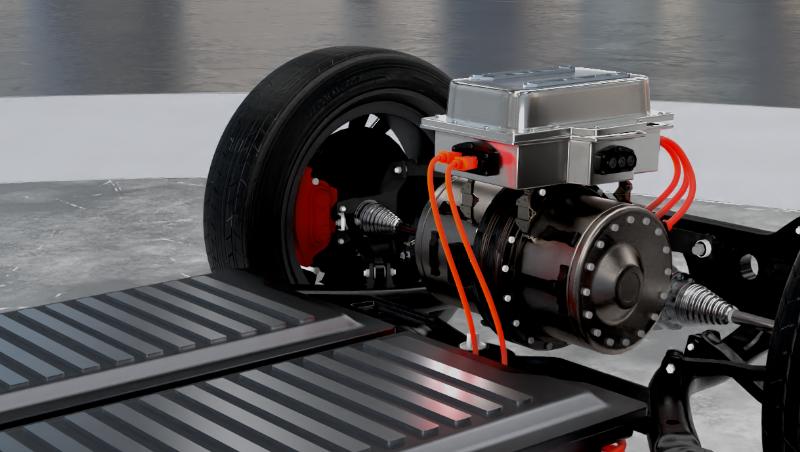
The role of the traction inverter is to convert the high-voltage DC from the EV battery to the AC required by the motor. The traction inverter controls the speed and torque of the motor, and its efficiency directly impacts the EV’s output power, thermal performance, and range. Figure 1 shows some of the most important chips or modules of a traction inverter: the microcontroller (MCU), isolated gate driver, and isolated bias power supply. To maximize the reliability and efficiency of your traction inverter, you must address the design challenges associated with these three components. Let’s take a look at this engineering science article on innovations that could help alleviate these challenges.

Figure 1 Block diagram of the electric vehicle traction inverter
Real-Time Control MCUs
Reducing the size and weight of electric vehicle traction inverters can increase range and reduce costs, which requires continuous innovation in MCUs. One way to reduce size and weight is to rotate the motor at higher speeds (>20 kRPM), which requires optimizing the control loop for low latency, from analog-to-digital converter (ADC) reads to field orientation control (FOC) calculations, as well as pulse width modulation (PWM) techniques.
TI has several accelerators and features to achieve low control loop latency, including several hardware accelerators designed specifically for traction inverters. two of the accelerators on the AM263P4-Q1 MCU are the resolver digitizer (RDC) and the trigonometric maths unit (TMU).
The RDC converts the sine/cosine feedback from the resolver sensor into velocity and position. This calculation is performed in dedicated hardware to speed up the conversion process and offload this functionality from the main core. additional diagnostics built into the TI MCU include sin 2 + cos 2 = 1 checks. Combining these diagnostics with two redundant RDCs creates an optimized solution for the traction inverter, which must meet automotive safety integrity level ASIL D. The TMU coprocessor works with each of the TMU co-processors to create an optimized solution for the traction inverter.
The TMU co-processor runs in parallel with each core and offloads the trigonometric functions from the main core, while also providing up to an 8x speed improvement. The speed improvement provides a significant control loop advantage for traction inverters, as most traction inverter control loops use FOC algorithms to implement the Clarke and Park transforms, which require trigonometric functions. The RDC and TMU accelerators, including the control subsystem, achieve real-time control latency of 3 µs, enabling control of high-speed traction inverter motors well above 20 kRPM, thereby reducing system size. The RDC and TMU accelerators (including the control subsystem) enable real-time control delays of 3 µs, enabling control of high-speed traction inverters well above 20 kRPM, thus reducing system size and weight.
Gate Drivers
With traction inverter power levels approaching 500 kW, improving efficiency (reducing energy loss throughout the drive cycle) is a major consideration in gate driver design. Other design requirements include power density, weight, height, functional safety, and cost.
To improve efficiency, silicon carbide (SiC) field effect transistors (FETs) are widely used. At the same time, switch-powered isolated gate drivers are becoming more sophisticated and now include isolated ADC sensing, multiple overcurrent protection modes, bias supply monitoring, gate monitoring, programmable safety states, built-in self-test, and a new feature called “real-time,” which is time-varying gate drive strength.
Depending on the safety requirements of the system, having gate driver integrated circuits (ICs) that are functionally safe and compliant can help support the system in achieving ISO 26262 compliance. For example, gate drivers can help to ensure ASIL-D fault detection rates of ≥99 percent for single faults and ≥90 percent for potential faults.
Modern gate driver ICs minimize the time component (dt) by turning SiC FETs on and off as quickly as possible through a voltage transition rate control method (transient voltage), reducing on and off energy and thus overall switching losses. This ability to control and vary the gate drive current strength significantly reduces switching losses, but at the cost of increasing transient overshoot at the node during switching, as shown in Figure 2.

Figure 2 The SiC conversion rate is controlled by changing the gate driver IC drive strength
Real-time variable gate drive strength provides the ultimate flexibility to optimize traction inverter designs to improve efficiency and mitigate transient overshoot. SiC transient overshoot reduction and efficiency optimization are possible regarding EV battery charging cycles, with three-quarters of a charging cycle available for efficiency improvements; see Figure 3. The functional safety-compliant UCC5880-Q1 gate driver can be configured for modification via the 4MHz bidirectional Serial Peripheral Interface (SPI) bus or the three digital input pins (you do not want to use the SPI bus to set the drive strength at power-up) The Q1 gate driver can be configured via the 4MHz bi-directional serial peripheral interface (SPI) bus or via three digital input pins (do not want to use the SPI bus to set drive strength at power-up).

Figure 3 Efficiency zone during battery peak voltage and charging state
Bias Power
Electric vehicles require efficient power conversion from traction inverters to achieve longer battery run times per full discharge cycle. Isolated gate driver bias supplies achieve high efficiency by minimizing conducted power losses in SiC power modules. Setting the gate voltage to the maximum allowable level reduces the drain-source on-resistance (RDS(on) ) while ensuring reliability (Figure 4). Lowering the RDS(on) is important when the current in the traction inverter is approaching and exceeding 400 A, as higher resistance results in high conduction power losses.

Figure 4 SiC Gate source voltage limit and conduction loss during the switching cycle
TI’s isolated DC/DC bias modules minimize conduction losses, while the UCC5880-Q1 minimizes switching losses. For SiC or IGBT drivers, positive and negative gate drive rail voltages can be easily adjusted to the most efficient gate voltage setting, with a 1.3% error over the full range of operating conditions (voltage, safe operating area power, temperature, and process). Closed-loop feedback provides highly accurate regulation for gate drive voltage control, maximizing the safety and efficiency of SiC or insulated gate bipolar transistor modules.
TI’s isolated DC/DC bias modules provide a high-density solution that integrates an isolated power transformer, primary-side bridge, secondary-side bridge, and control logic. The small package footprint enables efficient, compact drive solutions in multiphase traction inverters, reducing failure rates by reducing PCB area by more than 30 percent to less than 4 mm in height and eliminating more than 30 discrete components (Figure 5).

Figure 5 The TI isolation bias module is compared with the reverse excitation power supply size and components
Conclusion
With TI’s products, it is possible to improve the operating efficiency of next-generation traction inverters by up to 5 percent and achieve higher speeds, higher power density, lower height, lighter weight, and lower system cost. As the electric vehicle market accelerates, traction inverters will also gain continued attention.


Leave a comment