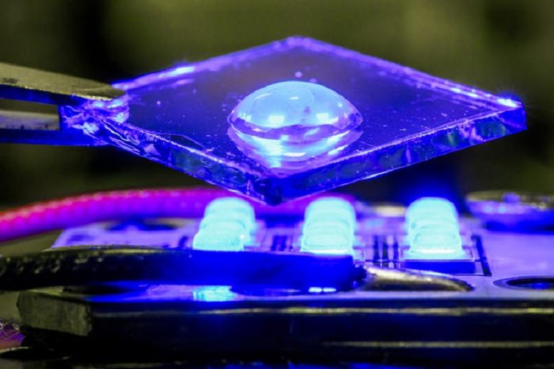
The new method involves immersing conductive plastic in a special salt solution (a photocatalyst) and then irradiating it with light for a short period to form p-doped conductive plastic, in which the only substance consumed is oxygen in the air.
Researchers at Linköping University in Sweden have developed a new method to make organic semiconductors more conductive with the help of air as a dopant. The study, published in the latest issue of the journal Nature, is an important step towards the future production of cheap and sustainable organic semiconductors.
Simone Fabiano, an associate professor at Linköping University, said this method could significantly affect how organic semiconductors are doped. All components in the new process are affordable, readily available, and environmentally friendly, which is a prerequisite for sustainable electronics in the future.
Organic semiconductors are used in digital displays, solar cells, LEDs, sensors, implants, and energy storage. To increase conductivity and improve semiconductor properties, dopants are often introduced. These dopants promote charge movement within the semiconductor material and can be tailored to induce positive (p-doping) or negative (n-doping) charges. The most common dopants currently in use generally have the disadvantages of being very reactive (unstable), expensive, and difficult to manufacture.
Now, researchers have developed this method of doping that can be performed at room temperature, in which an inefficient dopant (e.g., oxygen) is the primary dopant and light activates the doping process, which then facilitates the transfer of electrons from the inefficient dopant to the organic semiconductor material.
The new method is inspired by nature, as it shares many similarities with photosynthesis. Specifically, the conductive plastic is first immersed in a special salt solution (a photocatalyst) and then illuminated with light for a short period. The duration of the illumination determines the degree of doping of the material. Afterward, the solution is recycled for future use, leaving a p-doped conductive plastic in which the only substance consumed is oxygen in the air.
The researchers say the photocatalyst acts as an “electron shuttle” that can take electrons or deliver them to the material in the presence of a sacrificial agent. This is common in chemistry but has never been used in organic electronics.
Semiconductors based on conducting plastics rather than silicon have many potential applications, and dopants are key to enhancing their performance. The highlight of this study lies in the dopant. The ability to use both p- and n-doping in the same reaction is unique and simplifies the production of electronic devices, especially those that require both p- and n-doped semiconductors, such as thermoelectric generators. All components can be fabricated and doped at the same time, rather than one by one, making the process more scalable.


Leave a comment