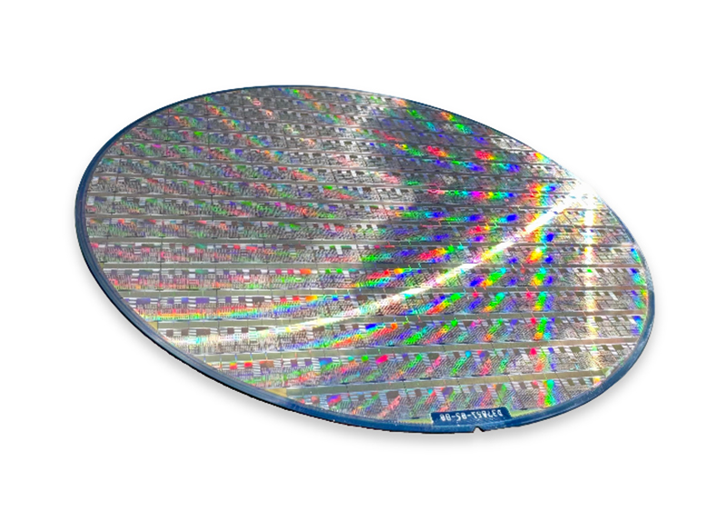
X-FAB Silicon Foundries, a leading global analog/mixed-signal semiconductor foundry group, announced the availability of its Gallium Nitride-on-Silicon foundry service for dMode devices, based on its XG035 technology platform, leveraging its expertise in Gallium Nitride processing for high-power applications. This move further utilizes and strengthens X-FAB’s position as a specialty pure-play foundry, now offering a complete portfolio of processing technologies covering GaN and other wide bandgap semiconductor materials (including Silicon Carbide), assisting fabless semiconductor companies in bringing their designs to life.
X-FAB’s GaN-on-Si technology is provided by its advanced 8-inch wafer fab in Dresden, Germany. This facility is one of six production sites X-FAB operates globally, featuring a stable and reliable manufacturing environment certified to automotive industry standards, equipped with various specialized processing equipment, measurement tools, and technologies optimized for GaN R&D and production, while also supporting analog CMOS processes. It can supply the thicker GaN-on-Si wafers required by customers in the automotive, data center, industrial, renewable energy, and medical fields.

Benefiting from years of deep accumulation in high-voltage GaN technology, following the recent announcement of opening the XG035 dMode process platform, X-FAB has now extended its internal expertise to dMode device GaN-on-Si foundry services. This process includes dMode HEMT transistors (voltage scalable from 100V to 650V) commonly used in power conversion applications. Furthermore, X-FAB can also provide customized GaN technologies and products, including dMode, eMode HEMTs, and Schottky Barrier Diodes, which are widely used in areas such as high-frequency rectification, power supply systems, and solar panels.
Global market demand for applications like charging equipment, electric vehicles, advanced energy management systems, and more powerful data centers continues to grow. In the case of data centers, the training and deployment of Artificial Intelligence are driving increasing demand for computing resources, which in turn fuels the need for higher power and more efficient electrical energy transmission and conversion technologies.
GaN-on-Si technology is a highly promising semiconductor industry that enables high-frequency switching and low on-resistance (Rds, the resistance between drain and source). With its small size and high-voltage handling capability, GaN-on-Si technology further completes X-FAB’s wide bandgap chip process portfolio, enabling customers to design more energy-efficient products from the grid level to automotive batteries and even down to the GPU level.
“We have over 30 years of experience in automotive-grade CMOS technology—including 350nm CMOS processes, shared tools and equipment, and BEOL—which gives our GaN technology inherent quality advantages and significantly lowers the customer entry barrier,”said Michael Woittennek, CEO of X-FAB Dresden. “We have been developing customized technologies for years, and now we are opening the XG035 dMode technology platform for general prototyping projects at our Dresden facility, located in the heart of the Silicon Saxony region. The flexibility of our 350nm toolset also allows us to quickly ramp up volume production, providing customers with a fast and reliable path to market.”
“As the GaN supplier landscape continues to evolve, X-FAB is progressively developing into a specialized GaN foundry partner,” added Luigi Di Capua, Vice President of Product Marketing at X-FAB. “Our 8-inch GaN-on-Si platform can help customers secure their supply chain and scale their designs with confidence.”
According to the latest news, X-FAB has already released a PDK (Process Design Kit) to simplify the customer design process and enable a faster start. Additionally, starting in Q4 2025, public MPW (Multi-Project Wafer) services will be opened, allowing multiple customers to share a single silicon wafer for chip fabrication. These initiatives will further lower the barriers to entry for prototyping and small-volume production.


