As the integrated circuit industry enters the “post-Moore era”, the difficulty and cost of improving the performance of integrated circuit chips are getting higher and higher, and there is an urgent need to find new technology solutions. Recently, the Shanghai Institute of Microsystems and Information Technology of the Chinese Academy of Sciences (SIIT) has made a breakthrough in the field of lithium tantalate heterogeneously integrated wafers and high-performance photonic chips and successfully developed a new type of mass-produced “optical silicon” chips. The latest research results were published online in the journal Nature on 8 May.
Currently, silicon optical technology and thin-film lithium niobate photonics technology as the representatives of integrated photonics technology is to deal with the performance of integrated circuits to enhance the bottleneck of the subversive technology. Among them, lithium niobate is known as “optical silicon”, which has received widespread attention in recent years, and foreign research institutions such as Harvard University have even proposed to build a new generation of “lithium niobate valley” modelled on the “Silicon Valley” model. “The programme.
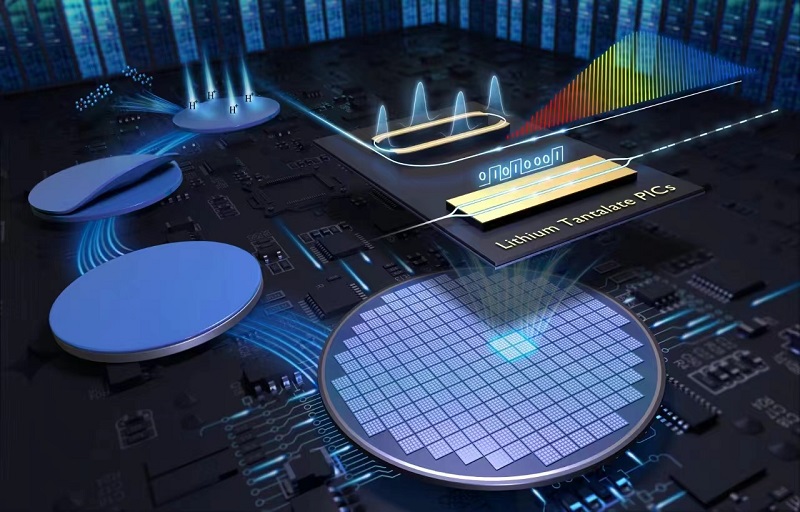
“Similar to lithium niobate, lithium tantalate can also be called ‘optical silicon’, and we and our co-authors have demonstrated that single-crystal lithium tantalate thin films also have excellent electro-optical conversion properties, and are even more advantageous than lithium niobate in some aspects.” Paper co-corresponding author, Shanghai Institute of Microsystems of the Chinese Academy of Sciences researcher Ou Xin said, more importantly, the preparation process of silicon-based lithium tantalate heterogeneous wafers is much closer to that of silicon wafers on insulators, so lithium tantalate films can be fabricated at low cost and on a large scale, which has a very high value of application.

This time, the scientific research team based on the “universal ion knife” heterogeneous integration technology, through the combination of ion implantation wafer bonding method, the preparation of high-quality silicon-based lithium tantalate single-crystal thin film heterogeneous wafers; at the same time, with the cooperation team jointly developed an ultra-low-loss lithium tantalate photonics device micro-nano-processing method, the success of the preparation of lithium tantalate photonic chips.
It is worth mentioning that the current research team has tackled 8-inch wafer preparation technology, for the development of a larger-scale domestic optoelectronic integrated chip and mobile terminal RF filter chip to lay the core material foundation.
Ou Xin said, the lithium tantalate photonic chip shows a very low optical loss, high efficiency electro-optical conversion and other characteristics, and is expected to break through the four major bottlenecks in the field of communication speed, power consumption, frequency, and bandwidth to provide a solution, and in the field of low-temperature quantum, optical computing, optical communications and other areas to give rise to revolutionary technologies.


